About Me
- I'm Alec, a 23-year-old physical design engineer from Chicago with a passion for building high-performance hardware systems
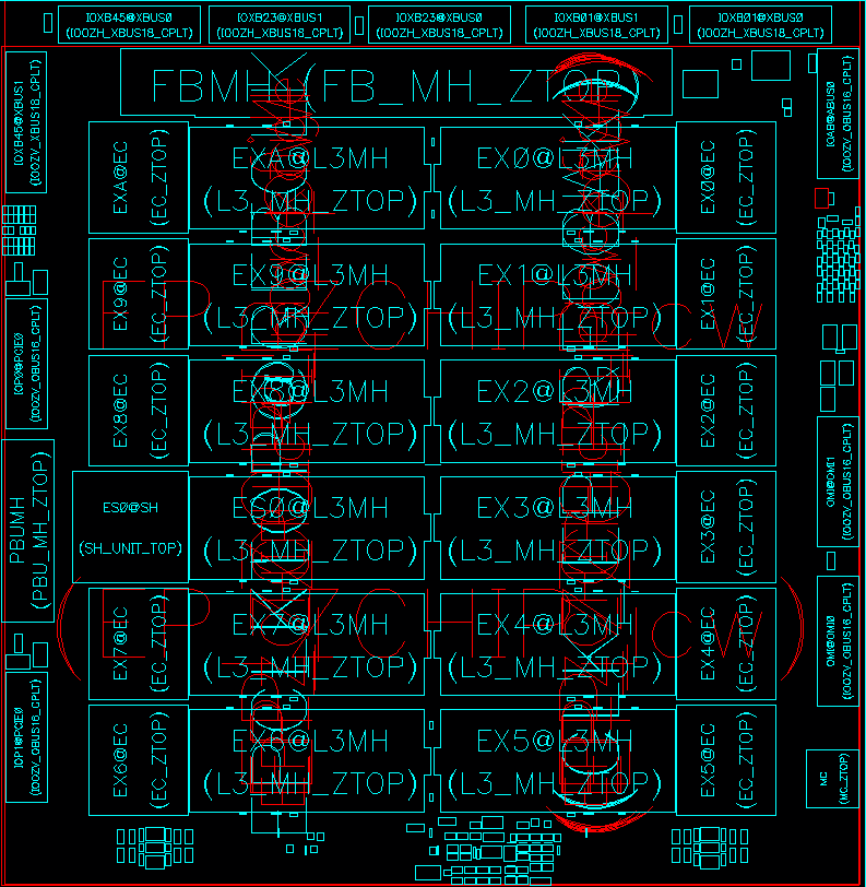
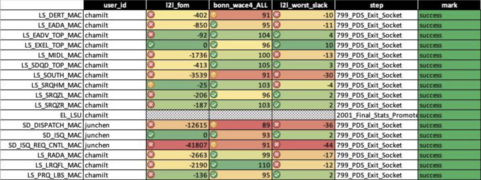
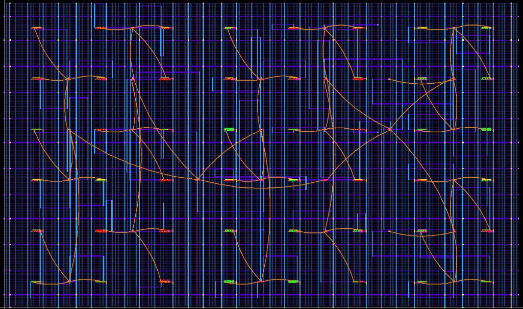
- Currently a CPU Physical Design & Integration Intern at IBM and pursuing an M.S. in ECE at Carnegie Mellon University, where I earned dual B.S. degrees in ECE and MSE
- I'm passionate about physical implementation—where form meets function at the nanoscale. I aim to design efficient, next-gen ASICs that push the limits of performance, power, and scalability
- I want to contribute to architectures that define the future of computing
- In my free time, I'm a major American football enthusiast and part-time rowing coach